12.02.2025 • News
Fujifilm Ramps up Capacity for Semiconductor Materials in Belgium
Fujifilm plans to invest approximately €25 million to install new production facilities for chemical mechanical planarization (CMP) slurries, which are used in advanced semiconductors, as well as enhance existing facilities for photolithography-related materials at its site in Antwerp, Belgium.
This expansion aims to meet the growing demand for automotive and industrial semiconductors in Europe, the company said.
The new facility for CMP slurries will expand Fujifilm’s global network to a total of six, with further sites in the US, Taiwan, South Korea and Japan.
In addition, Fujifilm will enhance the production facilities for developer used in the photolithography process at the Belgium site. This will help the company meet the increasing demand for automotive and industrial semiconductors in Europe and respond to the high-quality requirements of its customers, Fujifilm said.
The new CMP slurry production facilities and the enhanced developer production facilities are both scheduled to start operation in the spring of 2026.
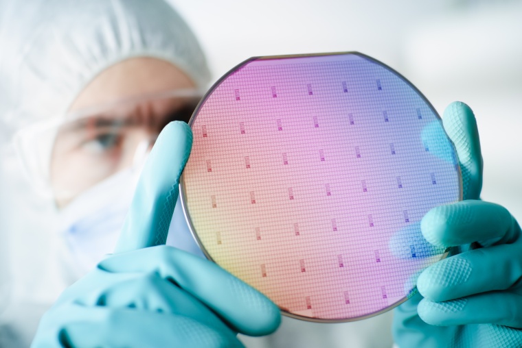
© Nicolas Loran/iStockphoto